

 Now that you've learned a little bit about Field Effect Transistors in general, and understand the basics behind how they work - lets discuss the major types of FET's you'll encounter in the field. The first of which is the JFET, or Junction Field Effect Transistor.
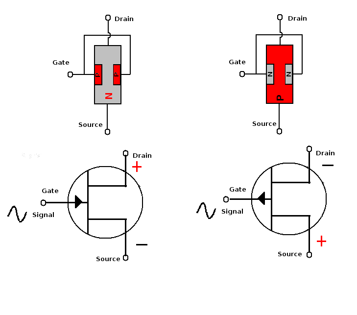
Like any other FET, the JFET has a gate, a source, and a drain, which corresponds to the base, emitter, and collector of a transistor (grid, anode, and cathode of a tube). It has a substrate and doping and a channel and a depletion region and all the other things that define what a Field Effect Transistor is. As we already discussed, the basic FET has no PN Junction for the electrons to jump across, like the standard "bipolar junction" transistor transistor does. Instead - the current flows through a channel, and as such, can actually flow in either direction (source to drain, or drain to source). This can cause problems in troubleshooting for beginners. This is because when you use an Ohmmeter to measure across the PN junction of a diode or Bipolar Junction Transistor (BJT), you'll see a high resistance in one direction, and a low resistance in the other. However on a JFET, you'll see about the same resistance from source to drain in either direction. Many times folks have replaced "bad transistors" because of this, only to find out that the new transistor read the same way - because it's not a BJT - it's a JFET! When electricity is applied to the oppositely doped gate - it generates an electromagnetic field within the device. That field causes the depletion region to expand or collapse, letting more, or fewer electrons pass through - hence the term "Field Effect". Another interesting feature of the JFET is its high input impedance, often thousands of Ohms. Typical transistors have a low input impedance (Rin), which means they have less sensitivity. The higher impedance and higher sensitivity comes at a cost though - they are more susceptible to static charges, and better care should be taken to avoid stray static, or they can be damaged before you even get them installed! But how exactly does a field effect transistor work in a real circuit? I thought you'd never ask! 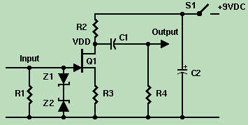 FET circuits work almost identical to Triode Tube circuits. The Source, Gate, and Drain act like the Anode, Grid, and Cathode respectively. As such, the R1 gate resistor acts like a grid resistor. The R3 source resistor acts like an anode resistor, and the drain resistor is the equivalent to a plate resistor as found in a vacuum tube circuit. With that thought in mind, FET's are used far more often in modern electronics, and are essentially the workhorse of any microprocessor chip. Now aren't you glad we spent so much time discussing tubes?
Vdd for this JFET is 9 Volts, which comes in at S1 and is applied to the drain of Q1 via the drain resistor R2. At this point you might ask why I called the 9 Volts coming in "Vdd"? Well, there are some "standard" names that we give to voltages in electroni circuits. For instance, Vdd, Vss, Vee, Vcc, Vgg, etc. These are usually easy to figure out. Vdd - drain voltage, Vcc, collector volgate, Vss source voltage, Vgg grid or gate voltage, etc. In addition, the same nomenclature applies to current, power, or resistance. Icc would be colector current, Rin - Input Resistance, Pout output power. I skimmed over this earlier in the course, but did not go into details. If you've arrived this far in the course - this should not be too difficult to comprehend. Once Vdd is applied to the drain of the FET, we have current flowing through the channel. Because it is a series circuit, all current flowing through the channel must also flow through R2, and R3. Let us assume that R3 is 560 Ohms, and R2 is 1.5K Ohms. That gives us (roughly) a resistance of 2.06K. 9 Volts divided by 2.06K Ohms (Remember Ohms Law?) gives us a current flow of about 4.36 mA. When we multiply times the resistance, we get the voltage, which winds up about a 6.55.2 volt drop across R2, and a 2.44 volt drop across R3. The values for R2 and R3 are chosen to keep the Vdd voltage roughly in the middle of the FET's rated range, so that it never goes into cutoff or saturation. Ratings for any particular FET can be found online. Did I lose you yet? Lets assume we chose an MPF102 or an NTE451 (Note: NTE makes equivalent components for almost any transistor or integrated circuit. They have an online cross reference that can be found at http://www.nteinc.com. This device has a (Max) 25Vdd. So with the maximum voltage in the circuit being 9V (our source battery voltage), we will never go into saturation for this inexpensive, high gain JFET. I would say we are operating in Class A mode. Our signal comes in on the gate, and out on the drain, meaning that the source is common to both input and output. So we say this is a Common Source, Class A Amplifier using an MPF102 JFET. Say that to your friends and they'll be impressed! Continuing with our circuit analysis, the voltage drop across R1 is nominally non existant - until you apply a signal at the input. The voltage vs ground is the voltage drop across R1 and the gate voltage (Vgg) at Q1. Note that the resistance of R1 is 3.3M&Ohm;. The resistance of R1 is chosen to keep the quiescent (silent/no signal applied) voltage at the drain midway between ground (0 Volts) and the highest possible voltage in the circtui (9 Volts). So typically, we have 4-5 volts at the drain with no signal applied. When we apply a signal to the gate of Q1, it swings positive and negative, changing the voltage drop (and current flow) through R1. The changing voltage coming into the gate opens and closes the depletion region of the JFET allowing more or less electrons to pass through from the source to the drain. This fluxuating current is seen by the drain resistor (Rdd). Since the Resistance of the resistor does not change, if we increase the current - it increases the voltage drop across the resistor. Likewise, if we decrease the current flow, we decrease the voltage drop. 9 volts is 9 volts. The source battery isn't going to change. So what happens to the voltage at Vdd when the voltage drop of the drain resistor changes? With 9 volts coming in, if there is only a 2 volt drop across the resistor, we have 7 volts at the Drain. On the flip side, if we have a 7 volt drop at the Drain resistor, we wind up with 2 volts at the Drain. So our output signal is swinging from 2 volts to 7 volts. So if this is all we need to get the JFET to amplify, what are all the other components for? Let's look at Z1 and Z2. Because the input signal to the JFET fluxuates, and COULD go above the ratings of the JFET (which is static sensitive), so a voltage clamping circuit, Zener Diodes Z1 and Z2, are put in place for protection of the amplifier. C2 is also for surge protection. As we flip the switch S1, a surge of current rushes in and can hurt our JFET. We put C2 there to soak up that surge, and keep the voltage coming into the circuit stable. C1 allows our output signal to pass through to the next circuit, while blocking any DC voltages from going to the next circuit (or coming from it). R4 is a "no load" load resistor. There may come a point when the amplifier is turned on, but no load is attached to it. If this is the case, then R4 protects the JFET from having its drain voltage go too high. Below is a list of components if you choose to build the circuit yourself and test it. It is a well designed, and fairly bullet proof circuit. Have Fun!
|
| (On The Following Indicator... PURPLE will indicate your current location) | ||||||||||||||||||||||||
| 1 | 2 | 3 | 4 | 5 | 6 | 7 | 8 | 9 | 10 | 11 | 12 | 13 | 14 | 15 | 16 | 17 | 18 | 19 | 20 | 21 | 22 | 23 | 24 | 25 |
| 26 | 27 | 28 | 29 | 30 | 31 | 32 | 33 | 34 | 35 | 36 | 37 | 38 | 39 | 40 | 41 | 42 | 43 | 44 | 45 | 46 | 47 | 48 | 49 | 50 |
| 51 | 52 | 53 | 54 | 55 | 56 | 57 | 58 | 59 | 60 | 61 | 62 | 63 | 64 | 65 | 66 | 67 | 68 | 69 | 70 | 71 | 72 | 73 | 74 | 75 |
[COURSE INDEX] [ELECTRONICS GLOSSARY] [HOME]
| Otherwise - please click to visit an advertiser so they know you saw their ad! |
